Low Noise DC Voltage Source
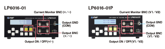
Low Noise DC Voltage Source LP6016-01/LP6016-01P
Bias-voltage and control-voltage source for sensors and devices
![]()
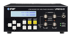
▲ LP6016-01

LP6016-01/LP6016-01P is a low voltage DC voltage source
equipped with LAN/USB/RS-232 interface.
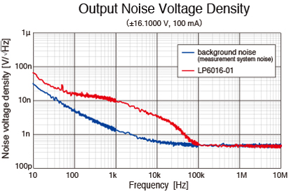
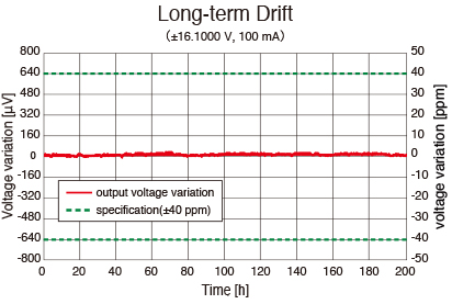
The output noise voltage is extremely small with a maximum of 10 μVrms, and the temperature stability of the output is
excellent at less than ±10 ppm/°C.
It can be used as a DC bias source for photodiodes and a control voltage source
for crystal oscillators.
Please refer to "Applications" page for further information.
2U,Half-rack size
Output Noise: 10 μVrms Bandwidth 10 Hz to 20 MHz
Output Voltage Stability: ±10 ppm/°C typical
Output voltage:
LP6016-01: 0 to +16.1 V (Positive), 0 to -16.1 V (Negative)
Positive and negative settings can be selected from tracking mode
or
independent mode.
LP6016-01P: 0 to +16.1 V (Dual Voltage Output / V1, V2)
V1 and V2 settings can be selected from tracking mode or
independent mode.
Setting resolution: 500 μV*
Setting accuracy: ±(0.03% +250 μV)*
Maximum current: 100 mA
Interface: USB, RS-232, LAN
*Modifications of setting
resolution and accuracy are available upon requests prior to placing your
orders.
Please
don’t hesitate to ask for details and pricings.
Modification
example,
Setting
Resolution: 100 µV
Setting
Accuracy: ±(0.03% +75 µV)
Applications
Improved Stability of Voltage Controlled Crystal Oscillator
Phase noise, frequency accuracy and frequency stability are normally measured during performance evaluation for crystal oscillators’ high performance voltage controlled devices such as VCXO, TCXO and OCXO, they are typically susceptible by noise and stability of their control voltage.
*VCXO (Voltage Controlled Crystal Oscillator), TCXO (Temperature Compensated Crystal Oscillator), OCXO (Oven Controlled Crystal Oscillator)
VCXO frequency measurement---different control voltage sources
A low
noise and stable control voltage source is used to
evaluate voltage control devices.
In the block diagram below, the output noise was measured with a general linear
power supply or LP6016-01 as the control voltage source.
Measurement Conditions
· - TCVCXO Center Frequency: approx. 30 MHz;
· - Measurement Cycle: 1 Hz;
· - Number of Measurements: 40,000 times;
· - Total Measurement Time: approx. 11 hours;
· - Ambient Temperature: 23 ±5°C.
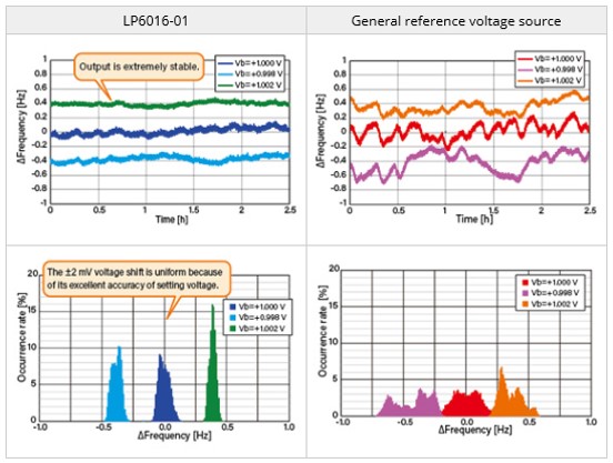
The upper part of the graph is the time change of the output frequency. When the LP series is used, the output frequency is stable for a long time.
The bottom part of the graph is a histogram display of the output frequency. The deviation from the center frequency is way smaller with our LP Series.
As we can see, the LP series is able to supply a stable voltage for a long time. A stable control voltage source is required to evaluate not only crystal oscillators but also voltage control components.
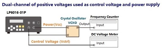
Measurement Block Diagram
Dual-channel of positive voltage are used for control voltage and power supply.
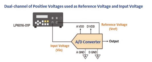
Reference voltage source for A/D converter
The reference voltage of the A/D converter affects the conversion accuracy, and the voltage noise and fluctuations are related to output performance. A low noise and stable voltage source is required for performance testing of A/D converters.
Output voltage of A/D converter---Difference between control voltage sources
In the block diagram below, the output voltage was measured when two different voltage sources were used, while the A/D converter reference voltage is at 4.096V and the input voltage is at 2.5V (≈ full scale).
Measurement Conditions
The output voltage is applied 80 million times in 80 minutes, and the variation is displayed in a histogram.
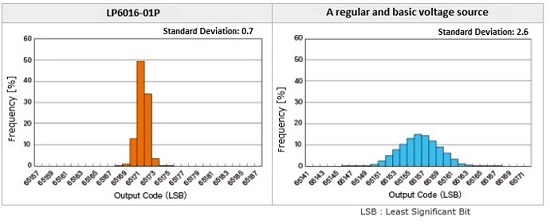
When the LP series is used, the variation in the LSB of the AD converter was reduced.
Measurement Block Diagram
Dual-channel of positive voltage are used for control voltage and power supply.
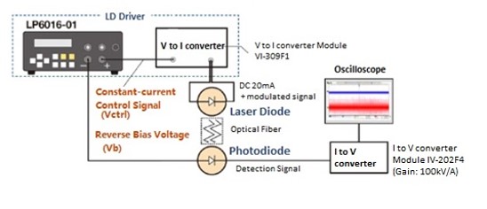
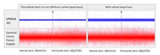
Improvement of S/N Ratio of Photodiode Output
When using a highly sensitive sensor, the noise of from its power source would affect the sensor's sensitivity. With different bias power sources applied to the photodiode, the output S/N ratios are compared below.
Video :
Photodiodes are widely used as light receiving elements for lasers, and in order to increase its sensitivity, a reverse bias voltage (Vb) is applied. A low-noise bias voltage source is required for sensitive photodetection.
Detection Signal Comparison---Difference Between Drive Power Supply and Bias Voltage Source
The detection signals were compared between the drive power supply (constant current control) and the bias voltage source using LP6016-01 or a general linear power supply.
Measurement Block Diagram
The positive voltage is used as the drive power supply and the negative voltage is used as the reverse bias power supply.